Silicon Substrate
Silicon single crystals are used as a semiconductor material, high-power transistor, rectifier, solar cells, etc.
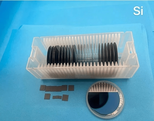
OST Photonics offers high quality Silicon substrates for researchers and industries. Crystal orientation, size and thickness can be customized according to your requirements.
Features
Low cost
Safe and non-toxic
Excellent machinability
Large size available
Applications
Integrated circuits
Semiconductor device
Consumer electronics
Solar cell substrate
Processing Capability
Orientation: <100>,<111>,<110>, etc.
Dimension: 2”, 3”, 4”, 5”, 6”, 8”, 12”, 5x5mm, 10x10mm, 20x20mm etc.
Thickness: 279 μm, 380 μm, 525 μm, 625 μm, 675 μm, 725 μm, 775 μm, 500 μm, 1000 μm etc.
Available items: wafers, substrates, blanks and customized optics
Specification and Properties of Silicon Substrates
Crystal Structure | Cubic | ||
Melting Point | 1420 ℃ | ||
Density | 2.4 g/cm3 | ||
Dopant | Undoped | Boron | Phosphorus |
Conduction type | Intrinsic | P-type | N-type |
Resistivity | >1000 ohm.cm | 0.001~1000 ohm.cm | 0.001~1000 ohm.cm |
EPD | ≤100 ∕cm2 | ≤100 ∕cm2 | ≤100 ∕cm2 |
Oxygen content(∕cm3) | ≤1~1.8×10^18 | ≤1~1.8×10^18 | ≤1~1.8×10^18 |
Carbon content(∕cm3) | ≤5×10^16 | ≤5×10^16 | ≤5×10^16 |
Orientation | <100>,<111>,<110>, etc. | ||
Orientation Tolerance | ±0.5° or better | ||
Dimension | 2”, 3”, 4”, 5”, 6”, 8”, 12”, 5x5mm, 10x10mm, 20x20mm etc. | ||
Dimension Tolerance | ±0.1 mm or better | ||
Thickness | 279 μm, 380 μm, 525 μm, 625 μm, 675 μm, 725 μm, 775 μm, 500 μm, 1000 μm etc. | ||
Thickness Tolerance | ±0.025 mm or better | ||
Surface Finish | Single side polished (SSP)/Double sides polished (DSP) | ||
Package | Class 100 clean bag, Class 1000 super clean room | ||