SrTiO3 Substrate
SrTiO3 single crystal provides a good lattice match to most of the materials with Perovskite structure. It is an excellent substrate for the epitaxial film of HTS and many oxides. It has been used widely for special optical windows and as high quality sputtering target.
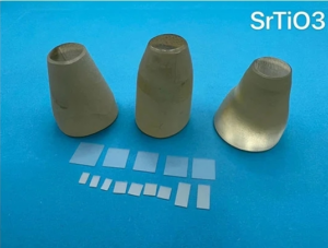
OST Photonics offers high quality SrTiO3 substrates for researchers and industries. Crystal orientation, size and thickness can be customized according to your requirements.
Features
Excellent physical and mechanical properties
Good lattice match to high-temperature superconducting materials such as YBa2Cu3O7
Applications
Substrate for the epitaxial film of HTS and many oxides
Special optical windows
Sputtering target
Processing Capability
Orientation: <100>,<110>,<111>, etc.
Dimension: 1”, φ30mm, 5x5mm, 10x5mm, 10x10mm, 20x20mm, etc.
Thickness: 0.5mm, 1.0mm, etc.
Available items: wafers, substrate, blanks, and customized optics
Specification and Properties of SrTiO3 Substrates
Crystal System | Cubic |
Growth Method | Verneuil technique, floating zone |
Crystal Lattice Constant | a=3.905 Å |
Melt Point | 2060 ℃ |
Density | 5.122 g/cm3 |
Hardness | 6-6.5 Mohs |
Thermal Expansion Coefficient | 9.4×10^-6 /℃ |
Dielectric Constant | ε=5.20 |
Chemical Stability | Insoluble in water |
Tangent Loss | ~5×10^-4 (300k) ~3×10^-4 (77k) |
Color | Transparent (sometimes slightly yellow according to the annealing state) |
Orientation | <100>,<110>,<111>, etc. |
Orientation Tolerance | ±0.5° or better |
Dimension | 1”, φ30mm, 5x5mm, 10x5mm, 10x10mm, 20x20mm, etc. |
Dimension Tolerance | ±0.1 mm or better |
Thickness | 0.5mm, 1.0mm, etc. |
Thickness Tolerance | ±0.05 mm or better |
Surface Finish | Single-side polished (SSP)/Double sides polished (DSP) |
Package | Class 100 clean bag, Class 1000 super clean room |