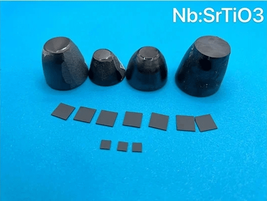
Nb:SrTiO3 Substrate
Niobium-doped strontium titanate has a similar structure to pure strontium titanate single crystal, but Nb:SrTiO3 has electrical conductivity. The conductive Nb:SrTiO3 substrates provide an electrode for certain thin film and device applications. At present, we can provide Nb:SrTiO3 single crystal substrates with Niobium doping concentration of: 0.1wt%, 0.5wt%, 0.7wt% and 1.0wt%.
OST Photonics offers high quality Nb:SrTiO3 substrates for researchers and industries. Crystal orientation, size and thickness can be customized according to your requirements.
Features
With superconductivity, semi-conductivity, gas sensitivity, heat sensitivity and photosensitivity
Low dielectric loss
High dispersion frequency
High dielectric constant
Applications
Nb:SrTiO3 substrates provide an electrode for certain thin film and device applications
Processing Capability
Orientation: <100>,<110>,<111>, etc.
Dimension: 1”, 10x5mm, 10x10mm, 15x15mm, 20x20mm, etc.
Thickness: 0.5mm, 1.0mm, etc.
Available items: wafers, substrates, blanks and customized optics
Specification and properties of Nb:SrTiO3 Substrates
Nb Concentration | 1.0wt% | 0.7wt% | 0.5wt% | 0.1wt% |
Resistivity | 0.0035 ohm.cm | 0.007 ohm.cm | 0.05 ohm.cm | 0.08 ohm.cm |
Mobility | 9.0 cm2/vs | 8.5 cm2/vs | 8.5 cm2/vs | 6.5 cm2/vs |
Orientation | <100>,<110>,<111>, etc. | |||
Orientation Tolerance | ±0.5° or better | |||
Dimension | 1”, 10x5mm, 10x10mm, 15x15mm, 20x20mm, etc. | |||
Dimension Tolerance | ±0.1 mm or better | |||
Thickness | 0.5mm, 1.0mm, etc. | |||
Thickness Tolerance | ±0.05 mm or better | |||
Surface Finish | Single side polished (SSP)/Double sides polished (DSP) | |||
Surface Roughness | Ra≤5Å (5µmx5µm) | |||
Package | Class 100 clean bag, Class 1000 super clean room | |||